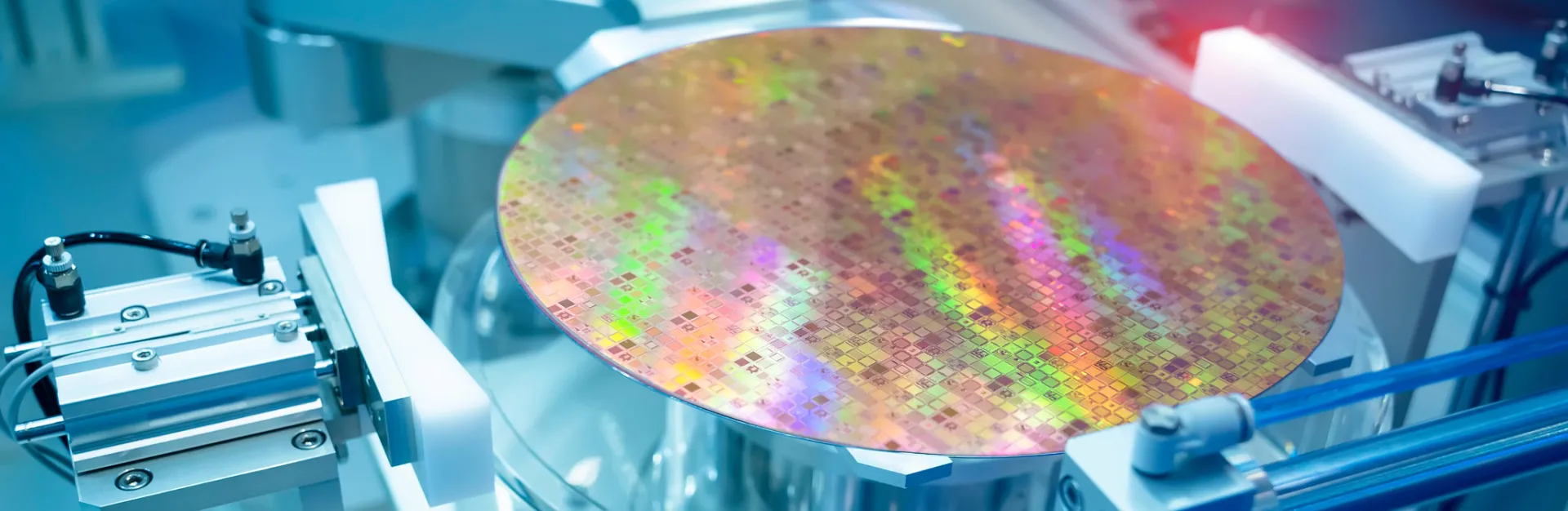
Semiconductors
Characterizing the Foundation of Electronic Properties
Powering Semiconductor Innovation: From Atoms to Devices
The modern world demands ever faster, more functional electronics devices, and so the components on which they rely must evolve at an ever fast rate. Semiconductors are becoming smaller, drawing less power and have improved bandwidth. But as microchips move ever closer to fundamental limitations because of their physical size, so the manufacturing difficulties increase.
Modeling & Simulation supports the development of these electronic components, from nanoscale semiconductors to flexible organic thin film transistors to bio-sensors by using electronic structure simulations as part of device design. As important is to increase the reliability of integrated circuits by modeling structural, electronic, thermal and mechanical properties of the materials.
A Complete Modeling & Simulation Toolset
BIOVIA Materials Studio provides a complete modeling & simulation toolset for exploring the key materials properties that underpin the function of semiconductors, transistors and photovoltaics.
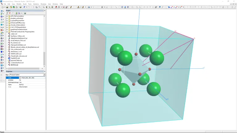
- Semiconductor Manufacturing
- Semiconductor Packaging
Semiconductor Manufacturing
- Elucidate the device characteristics defining electronic properties
- Determine the impacts of defects on performance
- Oxide-oxide interface evaluation
- ALD, CVD precursor evaluation and design
- Density of states and band gap (with offset) determination
- Photoresist analysis and gas diffusion analytics
- Electron transport to generate IV curve to help device design
- Optical properties for sensing capability
- Predict emission spectra for transistor materials for use in display technologies
- Designing thin-film transistors to conform effects of sputtering on crystal form
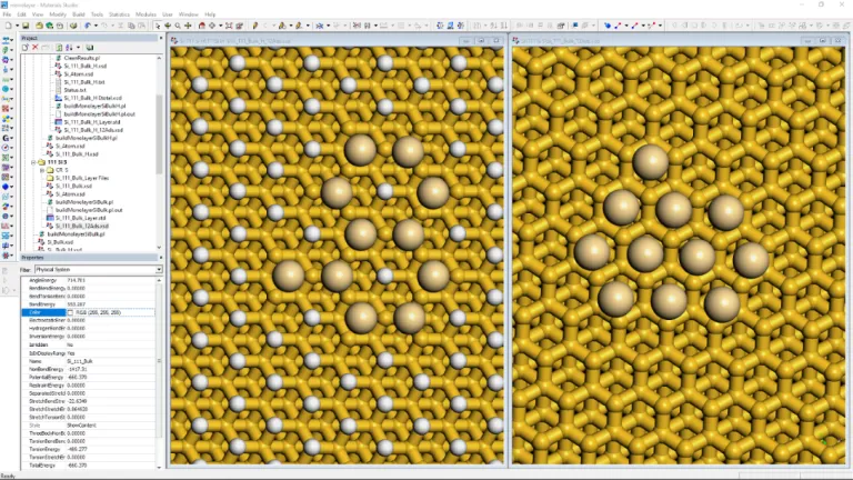
Semiconductor Packaging
- Determine the mesoscopic Heterogeneity in the curing process of resins to assess their thermal expansion during curing stages
- Calculate the adhesion of the epoxy resins with metal surfaces to address the issues of stability, moisture dependency
- Structural, and electronic property of solder joints
Explore Our Methods
The world of product development is changing. Discover how to stay a step ahead with BIOVIA.
Join the conversation in the BIOVIA Materials Studio User Community!
I am using BIOVIA Materials Studio (Forcite MD) to analyze a vapor/liquid system, where the liquid layer is in the middle of the cell. I want to calculate a density profile along the z-axis using the Concentration profiles in Forcite --> analysis. However, the liquid layer is moved along z-axis during MD runs, so the concentration cannot be calculated correctly. My question is how to remove such
BIOVIA MATERIALS STUDIO
BIOVIA TURBOMOLE 2026 HF1 was released in April 2026 and is available for download at https://software.3ds.com under BIOVIA products:Product line: Lab, Scientific and Content SolutionsRelease: 2026Level: BIOVIA 2026 GoldenFixes for this level: BIOVIA 2026 Golden HF3The following Technical Note informs you about BIOVIA TURBOMOLE 2026 HF1 including the release's supported operating systems, enhance
BIOVIA MATERIALS STUDIO
This script cycles through the physical systems in a Collection Document (XOD), switching the visibility of each physical system on and off. I combine it with screen capture tools to make videos that cannot easily be animated in a single trajectory document (ie cross-linking where the bonding changes, or processes where molecules are added or deleted).It can also be used to show lots of different
BIOVIA MATERIALS STUDIO
Also Discover
An Integrated, Multi-scale Modeling Environment
Foster Innovation with In Silico Design
Driving the Design of Advanced Composites and Polymers
Empowering Chemical & Catalyst R&D with BIOVIA Materials Studio

Supporting Metal Alloy Design with BIOVIA Materials Studio

Empowering the Virtual Design of Battery Materials and Fuel Cells
Driving the Virtual Design of Photovoltaics and Organic Electronics

Speeding up CPG R&D

Accelerating Pharmaceutical Development
Learn What BIOVIA Can Do for You
Speak with a BIOVIA expert to learn how our solutions enable seamless collaboration and sustainable innovation at organizations of every size.
Get Started
Courses and classes are available for students, academia, professionals and companies. Find the right BIOVIA training for you.
Get Help
Find information on software & hardware certification, software downloads, user documentation, support contact and services offering