
BIOVIA
Redefine the speed of R&D across biological, chemical, and material industries.
Generative AI for Every Scientist
Redefine how fast you can launch new products. Scientific AI gives every scientist cutting-edge generative technology to design faster, experiment virtually, and create more successful products through AI-powered Virtual Twins.
With a unified data model on an open, collaborative platform, thousands of companies use BIOVIA to bring new products to market faster than ever.
Feature Topics
Discover the world of BIOVIA
NVIDIA Partnership
Design the Impossible
Combine the power of NVIDIA-accelerated AI inference and BIOVIA’s world-class scientific AI and modeling. Discover the next generation of therapeutics and high-performance materials within a collaborative 3D UNIVERSE.
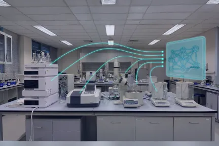
Create high-quality, AI-ready lab data from the start with a unified data model

Streamline Formula and Recipe Development Workflows on the 3DEXPERIENCE Platform

Achieve full digital transformation in your QC lab for faster, data-driven batch release processes.
Collaborate with BIOVIA experts to unleash the power of Gen AI and physics-based modeling and bring novel therapies to market faster.
News & Offers
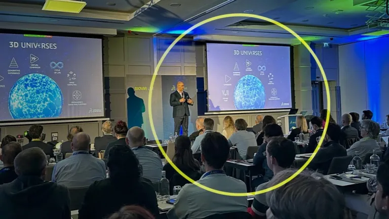
BIOVIA Live 2026
See how Scientific AI is transforming scientific discovery, product development, and manufacturing.

BIOVIA Scientific AI
Generative AI for scientific R&D advances innovation and helps scientists make better decisions.

BIOVIA Newsletter
Join to our monthly newsletter, and receive the latest information about our products, services, news and events.
Trusted by Industry Leaders
and thousands more.


Customer Stories
How Companies are Using our Scientific Research & Development Solutions
“We now have a paperless laboratory and can virtually simulate many of our experiments, minimizing materials consumption and waste, and accelerating the discovery of new natural healthcare products.”

BIOVIA Pipeline Pilot saved our scientists on average 1.5 hours per experiment and prevented errors in data transcription.

BIOVIA 3DEXPERIENCE Disciplines
Discover the Disciplines supported by our end-to-end portfolio, from design to manufacturing:

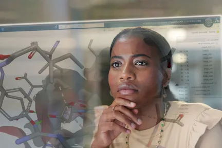
Accelerate Innovation in Life Sciences Research and Development

Optimize Lab Productivity and Compliance

Foster Innovation with In Silico Design

Transform Scientific Data into Knowledge

Reinventing Document Authoring with Structured Content

AI-based end-to-end digital Quality Management to ensure product quality and safety
BIOVIA Portfolio
Explore our Software and Solutions
Blog
Read the BIOVIA blog for valuable insight on the latest news and innovations from our experts.
From our Communities
Share your expertise and learn how other scientists and researchers solve problems with BIOVIA.
E-Seminars
E-books and Other Resources
BIOVIA Frequently Asked Questions
Connect with BIOVIA
Learn What BIOVIA Can Do for You
Speak with a BIOVIA expert to learn how our solutions enable seamless collaboration and sustainable innovation at organizations of every size.
Get Started
Courses and classes are available for students, academia, professionals and companies. Find the right BIOVIA training for you.
Get Help
Find information on software & hardware certification, software downloads, user documentation, support contact and services offering