
Semiconductor IP Management
Transform semiconductor innovation and engineering using design data governance as a competitive advantage
What is Semiconductor IP Management?
Semiconductor IP Management provides a unified approach to handling design data, intellectual property assets, requirements, changes and collaboration across the entire silicon lifecycle. Effective management scales IP reuse and maintains full traceability for complex System-on-a-Chip (SoC) development.
Without a governed environment, organizations struggle to keep pace with skyrocketing design complexity. This connected approach ensures that all stakeholders work from a shared, trusted source of information. It minimizes the risks of production delays, data silos and late-stage rework that can derail semiconductor delivery.
Semiconductor Innovation Through Intelligent IP Management
Semiconductor leaders are no longer competing on transistor density alone, but on how intelligently they manage, reuse and protect design data. As advanced nodes, chiplets, AI accelerators and automotive systems increase complexity, reusable IP and cross-domain dependencies continue to grow.
Traditional methods of managing design data and engineering processes can no longer keep pace. Semiconductor IP Management from Dassault Systèmes provides secure IP governance, structured change management, lifecycle traceability and cross-discipline collaboration across globally distributed teams and partners.
Streamline the Silicon Lifecycle with the 3DUNIV+RSES
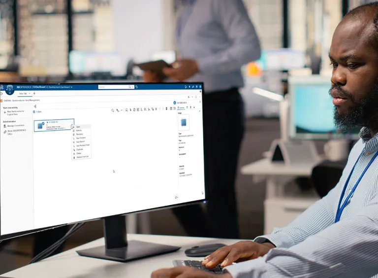
The 3DEXPERIENCE platform advances semiconductor IP management by providing a unified, governed environment where teams collaborate on product definitions in real time. It goes beyond a simple point solution by unifying design data, project execution and IP reuse on a single enterprise-ready foundation.
3D UNIVERSES build on the 3DEXPERIENCE platform foundations, connecting value networks with virtual twins and industrial AI. These virtual twin experiences enable teams to flexibly model, simulate and analyze semiconductor products and processes with the click of a button. This ensures that every aspect of the IP lifecycle is optimized for performance, quality and regulatory adherence, fostering innovation while mitigating risks.
Core Pillars of Semiconductor IP Management
Governed Semiconductor Lifecycle Management
Unify design data, IP reuse, requirements and change management in a governed Semiconductor environment. Enable digital continuity across complex SoC and chiplet programs with full traceability, controlled maturity states, scalable IP reuse, reduced rework and confident tape-out decisions.
Secure Collaboration & Automated Design Environment
Enable secure global engineering collaboration with automated provisioning, standardized design environments, and role-based access control. Reduce manual setup, configuration drift, IT overhead and IP leakage risks across multi-partner development programs.
Native EDA Integration
Keep engineers productive in native EDA environments with integrated revision control, Semiconductor item and IP management. Support Cadence, Synopsys, Git, GitHub, GitLab, Artifactory and DesignSync for repository-agnostic collaboration across diverse semiconductor workflows.
Sustainability and Semiconductor IP Management
Embed Sustainability Across the Product Lifecycle
Embedding sustainability into each stage of the semiconductor lifecycle—from initial concept to end-of-life—is essential for minimizing environmental impact and enhancing long-term business resilience. By integrating sustainability criteria directly into data-driven lifecycle workflows, engineering teams can make more informed decisions regarding materials selection, energy consumption and supply chain logistics.
Key Features of Semiconductor IP Management
Enterprise Governance
Ensure secure, compliant lifecycle control across teams and partners.
Accelerate Silicon Development
Reduce delays and streamline engineering workflows.
Improve Quality & Reduce Rework
Enable early alignment on requirements and changes.
Enable IP Reuse at Scale
Support governed reuse with full traceability.
Drive Engineering Velocity
Increase productivity through automation, visibility and collaboration.
Transforming Semiconductor Workflows for Modern Teams
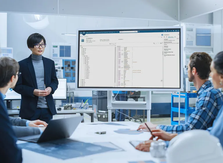
Managing complex multi-level SoC programs requires a modern, web-based experience for reviewing, validating and sharing design information. The 3DEXPERIENCE platform empowers Integrated Device Manufacturers (IDMs), fabless semiconductor companies and OEMs to design custom silicon with unprecedented clarity.
By maximizing data reuse and simplifying product structures early in the development phase, organizations reduce the time required to define the engineering baseline. Clear responsibilities and automated tool provisioning ensure compliance with organizational standards from the earliest stages of development.

Customer Stories
How Companies are Using ENOVIA Semiconductor IP Management
Airbus Helicopters
A key benefit is seeing how design changes affect the entire project. Engineers can trace how a modification in one area, such as an updated material property or new load condition, influences related simulations downstream. This gives them the confidence to decide whether further analysis is needed or if existing results remain valid.
Using the 3DEXPERIENCE platform to implement our SPDM solution was a no-brainer. We needed a single source of data that is accessible and shareable, where we can easily find and reuse the information we need.

FAQs- Semiconductor IP Management
Also Discover

Virtual Twins as the Next Generation of IP.

From legacy PLM repositories to supply aware, generative product definition for faster product realization

Maximize the efficiency and resilience of your semiconductor innovation chain through platform-based IP management.

Many of the greatest automotive innovations originate from the toughest, most competitive tests that vehicles are put through. These are all about staying ahead of the competition. The same is true for the automotive semi-conductor business. Taking part is simply not enough. So, how will you ensure that your business is a winner?
Learn What ENOVIA Can Do For You
Speak with an ENOVIA expert to learn how our solutions enable seamless collaboration and sustainable innovation at organizations of every size.
Get Started
Courses and classes are available for students, academia, professionals and companies. Find the right ENOVIA training for you.
Get Help
Find information on software & hardware certification, software downloads, user documentation, support contact and services offering.