eASIC
By using CST Studio Suite and partitioning the model, eASIC was able to achieve up to five-fold speed-up in its multi-level PCB and package simulations, when compared with simulation using the full model. This gave eASIC a significant speed advantage and helped them to shorten the design process.
Quick, Customizable Semiconductor Device Designs
eASIC is a fabless semiconductor company specializing in Single Mask Adaptable ASIC™ (application-specific integrated circuits). They produce custom integrated circuits for a wide range of applications, designed with the specific needs of the customers in mind. Supporting customers effectively, especially during the development stage of a new product, requires a rapid, cost-effective design and manufacturing process.
When designing a chip for a high-speed application, it’s not only the behavior of the IC itself that counts. The whole channel, including the package and the printed circuit board (PCB), affects the performance. By taking the PCB layout into account during the design stage, eASIC can improve the performance of the device and reduce the risk of problems emerging once installed.
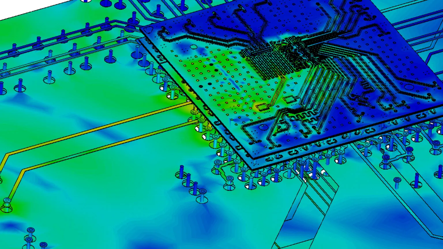
Simulating the Complex Package-PCB Interface
Electromagnetic simulation can allow the engineer to investigate the characteristics of a design before committing to manufacturing. Because PCBs are both large and complex while packages are small and intricate, modeling the entire system in one go is computationally intensive, requires long simulation times and heavy memory consumption. For this reason, eASIC decided to split the simulation, and model the package and PCB separately.
For this, eASIC chose CST Studio Suite, a full-wave 3D simulation tool. CST Studio Suite includes System Assembly and Modeling (SAM), which allows simulations to be linked and cascaded, so that the system can be considered as the sum of its parts. The existing combined package/PCB models were decomposed to separate the two parts, and were linked using ports with a reference plane at the interface.
Package-PCB co-design through a segmentation approach in CST Studio Suite, enabled us to leverage 3D EM simulation strength in an accurate analysis of the interconnect with model fitting on a cost-effective server machine in a reasonable run time. This is an amazing way to make full 3D simulation in complex designs a reality!”
Accurate Full-Wave Simulations in Half the Time
Compared to the simulation of the full model, the co-simulation using SAM was significantly faster and less computationally demanding. The co-simulation results matched both the full simulation results and actual measurements closely (Figure 3). Simulation was also able to accurately replicate widely-used laboratory measures such as time-domain reflectometry (TDR).
By using CST Studio Suite and partitioning the model, eASIC was able to achieve up to five-fold speed-up in its multi-level PCB and package simulations, when compared with simulation using the full model. This gave eASIC a significant speed advantage and helped them to shorten the design process.