
SIMULIA
Reveal the World We Live In
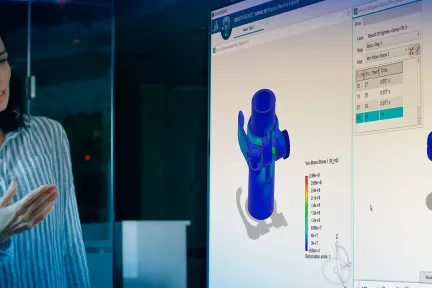
SIMULIA simulation software accelerates the process of evaluating the performance, reliability and safety of materials and products before committing to physical prototypes. Explore the engineering disciplines that we support.
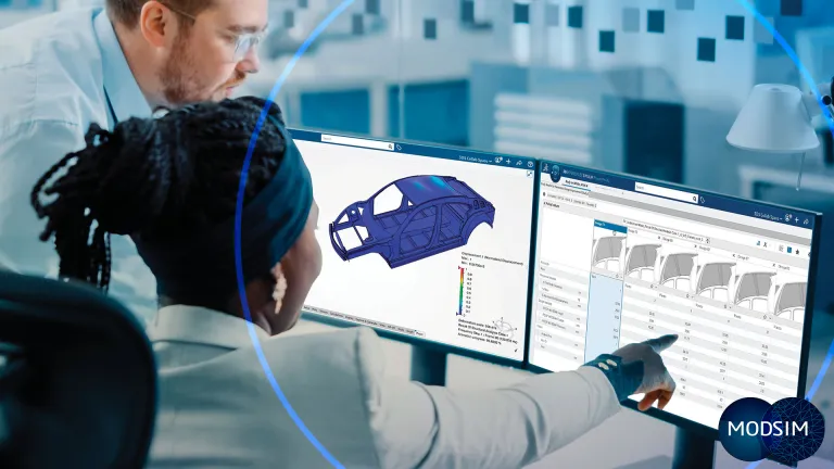
Finite Element Analysis for Mechanical and Civil Engineering
Simulation and Analysis of Electromagnetic Fields
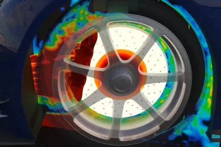
Steady-State and transient Internal and external flow around and through solids and structures
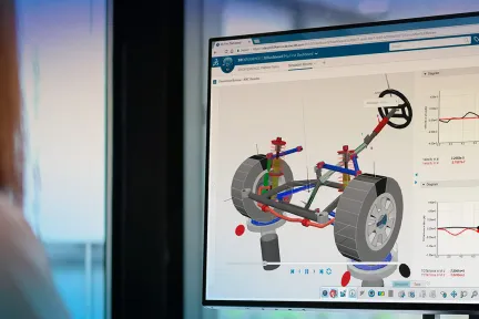
Analyse the Motion of Complex Mechanical Systems Under the Application of Mechanical Forces
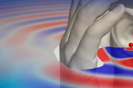
Simulation and analysis of noise and vibration across the entire audible frequency range
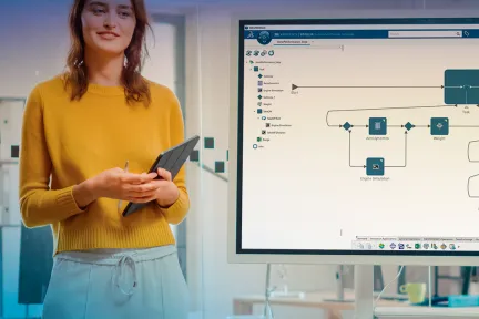
Democratize Simulation, Accelerate Innovation, and Take Advantage of the Power of Artificial Intelligence.
SIMULIA Portfolio
Explore our Software and Solutions
Featured Topics
Discover the world of SIMULIA
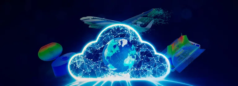
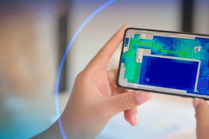
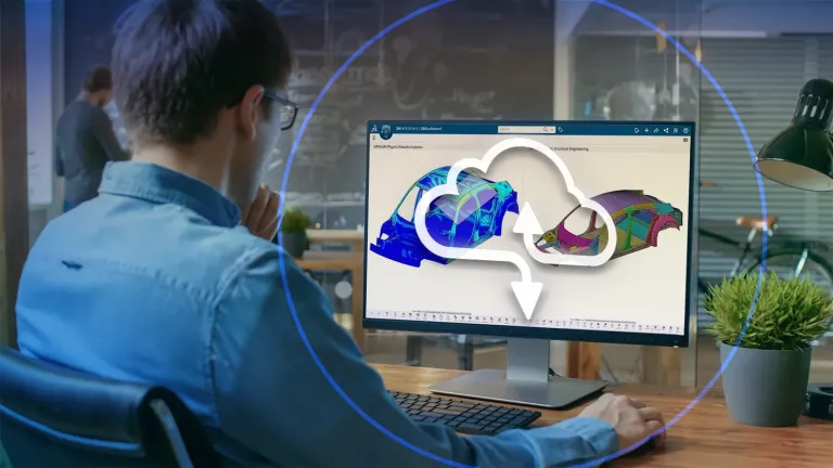
Reveal the Future With Simulation in the Cloud
Get more from your simulations and work more efficiently with AI-assisted performance-driven design with machine learning.

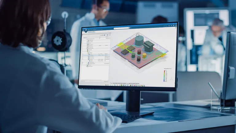
Simulation of Connected Systems and Devices Enables Efficient Product Design and Certification
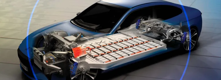
Simulations optimize EV design, enhance performance, and shape the future of sustainable transportation
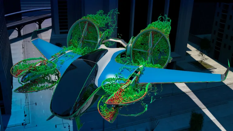
Simulation for Urban Air Mobility (UAM)
MODeling & SIMulation on the 3DEXPERIENCE platform
News & Offers
Accelerate Innovation with Scalable Simulation
Revolutionize product development with the 3DEXPERIENCE PLM Express. The AI-powered Design & Simulation Engineering bundles enable you to gain real-world insights and validate designs instantly.
Reduce prototyping expenses and boost product performance with smarter workflows, cloud-based solutions and generative AI.

Structural Simulation Newsletter
Learn more about our structural simulation product portfolio including the latest information on Abaqus for finite element analysis (FEA) as well as fe-safe for durability and fatigue evaluation.
Redefining Engineering Simulation in the Cloud - Webinar Series
We bring together leading experts from structural simulation, computational fluid dynamics, automation and optimization and electromagnetic simulation.
Customer Stories
How Companies are Using our Design & Engineering Simulation Solutions
Helix
The Next-Generation Electric Powertrains
Electric powertrain developer Helix has broken records and won awards for its high-performance electric motors and inverters. It is driving continuous improvements with 3DEXPERIENCE to achieve a finely tuned design and streamline engineering process from concept to manufacturing.
The 3DEXPERIENCE is at the center of everything we do in terms of design and then following through to production.

Events
E-Seminars
User Communities
Providing essential SIMULIA resources and active engagement with fellow users
SIMULIA Champions Program
The SIMULIA Champions Program pays tribute to our most active and influential simulation experts and brings them together to advance the future of simulation.
Our Champions are brand ambassadors who share their extraordinary expertise with other users, inspire peers, provide important feedback and enrich our SIMULIA community.
E-books and other Resources
Blogs
Read the SIMULIA blog on the latest news and innovations from our experts.
Connect with SIMULIA
Learn What SIMULIA Can Do for You
Speak with a SIMULIA expert to learn how our solutions enable seamless collaboration and sustainable innovation at organizations of every size.
Get Started
Courses and classes are available for students, academia, professionals and companies. Find the right SIMULIA training for you.
Get Help
Find information on software & hardware certification, software downloads, user documentation, support contact and services offering